Gerätedetails
Mask Aligner
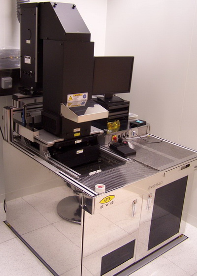
EVG 640
Mask Aligner
Photolithographie
EV Group
Photolithographie-Anwendungen in den Bereichen Advanced-Packaging, 3D-Packaging, MEMS, Interposer-Technologien, Fotovoltaik, Nanotechnologie und Wafer- und Board-Level-Optik
- Manual wafer load mask aligner
- Top Side Alignment (TSA), 10x microscope objectives
- Capable of Hard, Soft, Vacuum and Proximity Contact
- X, Y, Theta alignment with motorized linear stages
- Separation alignment: 5-400 µm (1 µm step)
- 3 point wedge compensation
- Configured for 8"/200 mm wafers (8"/200 mm wafer chuck)
- Maskholder: 5"x5", 9"x9" (with round and rectangular opening) and transparent (glass) holder for foil masks
- 1000 W Lamp House (16 mW/cm2 @ 356 nm)
- Vibration Isolation Table (built into system)
WHB 157
Back to list