Equipment Details
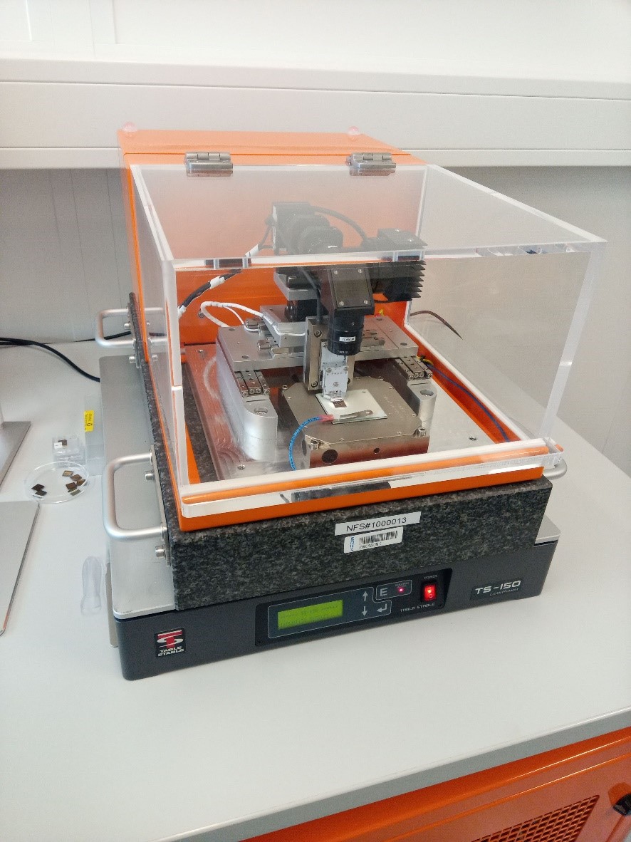
NanoFrazor
NANOFRAZOR SCHOLAR
Lithography
Photo lithography
Heidelberg Instruments
Nano-patterning in various application areas
Patterning performance
- Minimum structure size 20 nm
- Minimum lines and spaces (half pitch) 30 nm
- Writing field size (XY) 60 μm x 60 μm
- Write speed (50 nm pixel) 500 μm²/min
Imaging performance
- Lateral imaging resolution (feature size) 10 nm
- Vertical resolution (topography sensitivity) <0.5 nm
System features
- Substrate sizes 1 x 1 mm² to 100 x 100 mm²
FAM 346
Back to list